Non-strict and strict disjunction
Since the copula “or” is used in natural language in two meanings – connective-disjunctive and exclusive-disjunctive, then two types of disjunctive judgments should be distinguished: 1) non-strict (weak) disjunction and 2) strict (strong) disjunction.
Loose disjunction– a judgment in which the connective “or” is used in a connecting-disjunctive meaning (symbol ?). For example: “Melee weapons can be piercing or cutting” - symbolically R ? q. The connective “or” in this case separates, since such types of weapons exist separately, and connects, because there are weapons that simultaneously pierce and cut.
A loose disjunction will be true if at least one member of the disjunction is true and false if both its members are false.
Strict disjunction– a judgment in which the copula “or” is used in a disjunctive meaning (symbol– double disjunction). For example: “An act can be intentional or careless,” symbolically .
The terms of a strict disjunction, called alternatives, cannot both be true. If an act was committed intentionally, then it cannot be considered careless, and, conversely, an act committed through negligence cannot be considered intentional.
A strict disjunction will be true if one term is true and the other is false; it will be false if both terms are true or both terms are false. Thus, a proposition of strict disjunction will be true if one alternative is true and false if both alternatives are simultaneously false and true.
The disjunctive connective in language is usually expressed using the conjunctions “or”, “either”. In order to strengthen the disjunction to an alternative meaning, double conjunctions are often used: instead of the expression “p or q" use “either p or q”, and together “p or q"– “either p or q.” Since the grammar does not have unambiguous conjunctions for non-strict and strict division, the question of the type of disjunction in legal and other texts must be resolved by a meaningful analysis of the corresponding judgments.
Complete and incomplete disjunction
A disjunctive judgment is called complete or closed, which lists all the characteristics or all types of a certain kind.
Symbolically, this judgment can be written as follows: < р ? q ? r>. For example: “Forests are deciduous, coniferous or mixed.” The completeness of this division (in symbolic notation is indicated by the sign< … >) is determined by the fact that there are no other types of forests in addition to those indicated.
Incomplete, or open, is a disjunctive judgment that does not list all the characteristics or not all types of a certain kind. In symbolic notation, the incompleteness of a disjunction can be expressed by an ellipsis: R ? q ? r ? … In natural language, the incompleteness of a disjunction is expressed by the words: “etc.,” “etc.,” “and the like,” “others,” etc.
Notation for logical connectives:
negation (inversion, logical NOT) is denoted ¬ (for example, ¬A);
conjunction (logical multiplication, logical AND) is denoted by /\
(for example, A /\ B) either & (eg A & B);
disjunction (logical addition, logical OR) is denoted by \/
(for example, A \/ B);
following (implication) denoted by → (for example, A → B);
identity denoted by ≡ (for example, A ≡ B). The expression A ≡ B is true if and only if the values of A and B are the same (either they are both true, or they are both false);
character 1 (unit) is used to denote truth (true statement);
character 0 (zero) is used to indicate a lie (false statement).
Two logical expressions containing variables are called equivalent if the values of these expressions coincide for any values of the variables. Thus, the expressions A → B and (¬A) \/ B are equivalent, but A /\ B and A \/ B are not (the meanings of the expressions are different, for example, when A = 1, B = 0).
Priorities of logical operations: inversion (negation), conjunction (logical multiplication), disjunction (logical addition), implication (following), identity. Thus, ¬A \/ B \/ C \/ D means the same as
((¬A) \/ B) \/ (C \/ D).
It is possible to write A \/ B \/ C instead of (A \/ B) \/ C. The same applies to the conjunction: it is possible to write A /\ B /\ C instead of (A /\ B) /\ C.
Properties of logical operations
General properties of logical operations
For a set of n there are exactly logical variables 2n different meanings. The truth table for a logical expression of n variables contains n+1 column and 2n lines.
Disjunction
If at least one of the subexpressions to which the disjunction is applied is true on some set of values of the variables, then the entire disjunction is true for this set of values.
If all expressions from a certain list are true on a certain set of variable values, then the disjunction of these expressions is also true.
If all expressions from a certain list are false on a certain set of variable values, then the disjunction of these expressions is also false.
The meaning of a disjunction does not depend on the writing order of the subexpressions to which it is applied.
Conjunction
If at least one of the subexpressions to which the conjunction is applied is false on some set of variable values, then the entire conjunction is false for this set of values.
If all expressions from a certain list are true on a certain set of variable values, then the conjunction of these expressions is also true.
If all expressions from a certain list are false on a certain set of variable values, then the conjunction of these expressions is also false.
The meaning of a conjunction does not depend on the order in which the subexpressions to which it is applied are written.
Simple disjunctions and conjunctions
Let us call (for convenience) a conjunction simple if the subexpressions to which the conjunction is applied are different variables or their negations. Similarly, a disjunction is said to be simple if the subexpressions to which the disjunction is applied are distinct variables or their negations.
A simple conjunction takes on the meaning 1 (true) on exactly one set of variable values.
A simple disjunction takes on the meaning 0 (false) on exactly one set of variable values.
Implication
The implication A →B is equivalent to the disjunction (¬A) \/ B. This disjunction can also be written as follows: ¬A \/ B.
The implication A →B evaluates to 0 (false) only if A=1 and B=0. If A=0, then the implication A →B is true for any value of B.
Disjunction
Disjunction- (lat. disjunctio - disjunction) logical operation, in its application as close as possible to the union “or” in the sense of “either this, or that, or both at once.” Synonyms: logical "OR", including "OR", logical addition, sometimes just "OR".
Disjunction can be binary operation, that is, to have two operands, ternary operation, that is, to have three operands or n-ary operation, that is, to have n operands.
The entry may be prefix- the operation sign precedes the operands (Polish notation), infix- the operation sign is between the operands or postfix- the operation sign comes after the operands. When the number of operands is more than 2, prefix and postfix notations are more economical.
The most common recording options are:
|| | .
Boolean algebra
Definition.
Logic function MAX in two-valued (binary) logic is called disjunction (logical "OR", logical addition or simply "OR").
Rule: The result is equal to the largest operand.
Description.
In Boolean algebra, a disjunction is a function of two, three or more variables (they are also the operands of an operation, they are also the arguments of a function).
Rule: the result is equal if all operands are equal; in all other cases the result is equal to .
| Truth table | ||
|---|---|---|
Truth table for ternary (three-operand) disjunction:
| X | Y | Z | X Y Z |
|---|---|---|---|
| 0 | 0 | 0 | 0 |
| 1 | 0 | 0 | 1 |
| 0 | 1 | 0 | 1 |
| 1 | 1 | 0 | 1 |
| 0 | 0 | 1 | 1 |
| 1 | 0 | 1 | 1 |
| 0 | 1 | 1 | 1 |
| 1 | 1 | 1 | 1 |
Multi-valued logic
An operation called in binary logic disjunction, in multivalued logics is called maximum: , where , a is the meaning of logic. Other options are also possible. Typically, one tries to maintain compatibility with Boolean algebra for operand values.
It should be noted that the name of this operation maximum makes sense in logics with any value, including binary logic, and the names disjunction, logical "OR", logical addition and just "OR" make sense only in binary logic, and when moving to multi-valued logic they lose their meaning.
Classical logic
In classical propositional calculus, the properties of a disjunction are defined using axioms. The classical propositional calculus can be specified by different systems of axioms, and some of them will describe the properties of disjunction. One of the most common options includes 3 axioms for disjunction:
Using these axioms, you can prove other formulas containing the disjunction operation. Please note that classical propositional calculus does not calculate the result from the values of the operands (as in Boolean algebra), but rather requires proving the formula as a whole based on axioms and rules of inference. Flying high hurts falling
Circuit design
| 0 | 0 | 0 |
| 1 | 0 | 1 |
| 0 | 1 | 1 |
| 1 | 1 | 1 |
The mnemonic rule for a disjunction with any number of inputs is: The output will be:
- "1" if and only if at least on one there is a "1" in the input
- "0" if and only if everyone inputs "0"
Programming
There are two main types of disjunction used in computer languages: logical OR and bitwise OR. For example, in the C/C++ languages, logical “OR” is denoted by the symbol “||”, and bitwise “OR” is denoted by the symbol “|”. In the Pascal/Delphi languages, both types of disjunction are indicated using the keyword " or", and the result of the action is determined by the type of the operands. If the operands are of a logical type (for example, Boolean), a logical operation is performed; if the operands are an integer (for example, Byte), a bitwise operation is performed.
Logical "OR" is used in conditional jump operators or in similar cases where the result or is required. For example:
If (a || b) ( /* some actions */ } ;
The result will be equal if both operands are equal or . In any other case, the result will be equal to .
In this case, the standard convention applies: if the value of the left operand is equal to , then the value of the right operand is not calculated (a complex formula may be used instead). This convention speeds up program execution and is a useful technique in some cases. The Delphi compiler supports a special directive that includes
($B-)
or turning off
($B+)
similar behavior. For example, if the left operand tests whether the right operand needs to be evaluated:
If (a == NULL || a-> x == 0 ) ( /* some actions */ } ;
In this example, thanks to the check in the left operand, a null pointer dereference will never occur in the right operand.
Bitwise OR performs a normal Boolean algebra operation on all the bits of the left and right operand in pairs. For example,
| If | |
| a = | |
| b = | |
| That | |
| a OR b = |
Connection with natural language
The similarity between disjunction and the conjunction “or” in natural language is often pointed out when it is used in the sense of “either this, or that, or both.” In legal documents they often write “and/or,” meaning “either this, or that, or both.” A compound statement "A and/or B" is considered false when both statements A and B are false, otherwise the compound statement is true. This exactly corresponds to the definition of disjunction in Boolean algebra, if “true” is denoted by , and “false” by .
Ambiguity natural language is that the conjunction “or” is used in two meanings: either to indicate disjunction, or to indicate another operation -
PROPERTIES OF LOGICAL OPERATIONS
1. Designations
1.1. Notation for logical connectives (operations):
a) negation(inversion, logical NOT) is denoted by ¬ (for example, ¬A);
b) conjunction(logical multiplication, logical AND) is denoted by /\
(for example, A /\ B) or & (for example, A & B);
c) disjunction(logical addition, logical OR) is denoted by \/
(for example, A \/ B);
d) following(implication) is denoted by → (for example, A → B);
e) identity denoted by ≡ (for example, A ≡ B). The expression A ≡ B is true if and only if the values of A and B are the same (either they are both true, or they are both false);
f) symbol 1 is used to denote truth (true statement); symbol 0 – to indicate a lie (false statement).
1.2. Two Boolean expressions containing variables are called equivalent (equivalent) if the values of these expressions coincide for any values of the variables. Thus, the expressions A → B and (¬A) \/ B are equivalent, but A /\ B and A \/ B are not (the meanings of the expressions are different, for example, when A = 1, B = 0).
1.3. Priorities of logical operations: inversion (negation), conjunction (logical multiplication), disjunction (logical addition), implication (following), identity. Thus, ¬A \/ B \/ C \/ D means the same as
((¬A) \/ B) \/ (C \/ D).
It is possible to write A \/ B \/ C instead of (A \/ B) \/ C. The same applies to the conjunction: it is possible to write A /\ B /\ C instead of (A /\ B) /\ C.
2. Properties
The list below is NOT intended to be complete, but is hopefully representative enough.
2.1. General properties
- For a set of n there are exactly logical variables 2 n different meanings. Truth table for logical expression from n variables contains n+1 column and 2 n lines.
2.2.Disjunction
- If at least one of the subexpressions to which the disjunction is applied is true on some set of values of the variables, then the entire disjunction is true for this set of values.
- If all expressions from a certain list are true on a certain set of variable values, then the disjunction of these expressions is also true.
- If all expressions from a certain list are false on a certain set of variable values, then the disjunction of these expressions is also false.
- The meaning of a disjunction does not depend on the writing order of the subexpressions to which it is applied.
2.3. Conjunction
- If at least one of the subexpressions to which the conjunction is applied is false on some set of variable values, then the entire conjunction is false for this set of values.
- If all expressions from a certain list are true on a certain set of variable values, then the conjunction of these expressions is also true.
- If all expressions from a certain list are false on a certain set of variable values, then the conjunction of these expressions is also false.
- The meaning of a conjunction does not depend on the writing order of the subexpressions to which it is applied.
2.4. Simple disjunctions and conjunctions
Let us call (for convenience) the conjunction simple, if the subexpressions to which the conjunction is applied are distinct variables or their negations. Similarly, the disjunction is called simple, if the subexpressions to which the disjunction is applied are distinct variables or their negations.
- A simple conjunction evaluates to 1 (true) on exactly one set of variable values.
- A simple disjunction evaluates to 0 (false) on exactly one set of variable values.
2.5. Implication
- Implication A →B is equivalent to disjunction (¬ A) \/ B. This disjunction can also be written as follows: ¬ A\/B.
- Implication A →B takes the value 0 (false) only if A=1 And B=0. If A=0, then the implication A →B true for any value B.
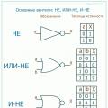
Logical operations. Disjunction, conjunction and negation
So how do simple logical statements connect with each other to form complex ones? In natural language we use various conjunctions and other parts of speech. For example, “and”, “or”, “either”, “not”, “if”, “then”, “then”. Example of complex statements: “he has knowledge And skills", "she will arrive on Tuesday, or on Wednesday", "I will play Then, when I do my homework", "5 Not equals 6". How do we decide what we've been told is true or not? Somehow logically, even somewhere unconsciously, based on previous life experience, we understand that the truth with the union “and” occurs in the case of the truthfulness of both simple statements. Once one becomes a lie, the entire complex statement will be false. But, with the connective “or”, only one simple statement must be true, and then the whole expression will become true.
Boolean algebra transferred this life experience to the apparatus of mathematics, formalized it, and introduced strict rules for obtaining an unambiguous result. Unions began to be called logical operators here.
The algebra of logic involves many logical operations. However, three of them deserve special attention, because... with their help you can describe all the others, and, therefore, use less variety of devices when designing circuits. Such operations are conjunction(AND), disjunction(OR) and negation(NOT). Often the conjunction is denoted & , disjunction - || , and the negation is a bar over the variable indicating the statement.
With a conjunction, the truth of a complex expression arises only if all the simple expressions that make up the complex are true. In all other cases, the complex expression will be false.
With disjunction, the truth of a complex expression occurs when at least one simple expression included in it is true, or two at once. It happens that a complex expression consists of more than two simple ones. In this case, it is enough for one simple to be true and then the whole statement will be true.
Negation is a unary operation, because it is performed in relation to one simple expression or in relation to the result of a complex one. As a result of negation, a new statement is obtained that is opposite to the original one.
Truth tables
It is convenient to describe logical operations by the so-called truth tables, which reflect the results of calculations of complex statements for different values of the original simple statements. Simple statements are denoted by variables (for example, A and B).
Logical Fundamentals of Computer
Computers use various devices, the operation of which is perfectly described by the algebra of logic. Such devices include groups of switches, triggers, adders.
In addition, the connection between Boolean algebra and computers lies in the number system used in the computer. As you know, it is binary. Therefore, computer devices can store and transform both numbers and the values of logical variables.
Switching circuits
Computers use electrical circuits consisting of many switches. The switch can only be in two states: closed and open. In the first case, the current passes, in the second - not. It is very convenient to describe the operation of such circuits using the algebra of logic. Depending on the position of the switches, you may or may not receive signals at the outputs.
Gates, flip-flops and adders
A gate is a logical element that accepts some binary values and produces others depending on its implementation. For example, there are gates that implement logical multiplication (conjunction), addition (disjunction) and negation.
Triggers and adders are relatively complex devices consisting of simpler elements - gates.
The trigger is capable of storing one binary digit, due to the fact that it can be in two stable states. Triggers are mainly used in processor registers.
Adders are widely used in processor arithmetic logic units (ALUs) and perform summation of binary bits.
The construction of computers, or rather hardware, is based on the so-called valves. They are fairly simple elements that can be combined with each other, thereby creating various schemes. Some schemes are suitable for implementation arithmetic operations, and on the basis of others they build different memory COMPUTER.
A ventel is a device that produces the result of a Boolean operation from the data (signals) entered into it.
The simplest valve is a transistor inverter that converts low voltage to high voltage or vice versa (high to low). This can be thought of as converting a logical zero to a logical one or vice versa. Those. we get the valve NOT.
By connecting a pair of transistors in different ways, gates are obtained OR NO And AND-NOT. These gates no longer accept one, but two or more input signals. The output signal is always the same and depends (produces high or low voltage) on the input signals. In the case of a NOR gate, a high voltage (logical one) can only be achieved if all inputs are low. In the case of an NAND gate, the opposite is true: a logical one is obtained if all input signals are zero. As you can see, this is the opposite of such familiar logical operations as AND and OR. However, NAND and NOR gates are commonly used because their implementation is simpler: AND-NOT and NOR-NOT are implemented by two transistors, while logical AND and OR are implemented by three.
The gate output can be expressed as a function of the inputs.
It takes very little time for a transistor to switch from one state to another (switching time is measured in nanoseconds). And this is one of the significant advantages of schemes built on their basis.

For logical values, three operations are commonly used:
- Conjunction– logical multiplication (AND) – and, &, ∧.
- Disjunction– logical addition (OR) – or, |, v.
- Logical negation (NOT) – not,.
Logical expressions can be converted according to laws of algebra of logic:
- Laws of reflexivity
a ∨ a = a
a ∧ a = a - Commutativity laws
a ∨ b = b ∨ a
a ∧ b = b ∧ a - Laws of associativity
(a ∧ b) ∧ c = a ∧ (b ∧ c)
(a ∨ b) ∨ c = a ∨ (b ∨ c) - Distributivity laws
a ∧ (b ∨ c) = (a ∧ b) ∨ (a ∧ c)
a ∨ (b ∧ c) = (a ∨ b) ∧ (a ∨ c) - Law of Negation of Negation
(a) = a - De Morgan's laws
(a ∧ b) = a ∨ b
(a ∨ b) = a ∧ b - Laws of absorption
a ∨ (a ∧ b) = a
a ∧ (a ∨ b) = a
Every logical formula defines some Boolean function. On the other hand, for any Boolean function one can write infinitely many formulas representing it. One of the main tasks of logical algebra is finding canonically x forms (i.e. formulas constructed according to a certain rule, canon), as well as the simplest formulas representing Boolean functions.
If a logical function is expressed through disjunction, conjunction and negation of variables, then this form of representation is called normal. Among normal forms, there are those in which functions are written in a unique way. They are called perfect.
A special role in the algebra of logic is played by the classes of disjunctive and conjunctive perfect normal forms. They are based on the concepts of elementary disjunction and elementary conjunction.
The formula is called elementary conjunction, if it is the conjunction of one or more variables, taken with or without negation. One variable or its negation is considered one-term elementary conjunction.
The formula is called elementary disjunction, if it is a disjunction (perhaps monomial) of variables and negations of variables.
DNF AND SDNF
The formula is called disjunctive normal form(DNF), if it is a disjunction of non-repeating elementary conjunctions. DNFs are written as: А1 v А2 v ... v Аn, where each An- elementary conjunction.
Formula A from k variables are called perfect disjunctive normal form(SDNF), if:
1.A is a DNF in which every elementary conjunction is a conjunction k variables x1, x2, …, xk, and in the i-th place of this conjunction there is either a variable xi or its denial;
2. All elementary conjunctions in such a DNF are pairwise distinct.
For example: A = x1 & NOT x2 v x1 & x2
A perfect disjunctive normal form is a formula constructed according to strictly defined rules up to the order of the elementary conjunctions (disjunctive terms) in it.
It is an example of a unique representation of a Boolean function in the form of a formulaic (algebraic) notation.
SDNF theorem
Let f(x1 x2, …, xn)– Boolean function of n variables that is not identically zero. Then there is a perfect disjunctive normal form expressing the function f.
Algorithm for constructing SDNF using a truth table:
1. In the truth table, we mark the sets of variables for which the value of the function f = 1.
2.For each marked set, we write the conjunction of all variables as follows: if the value of some variable in this set is equal to 1, then we include the variable itself in the conjunction, otherwise, its negation.
3. We connect all the resulting conjunctions with disjunction operations.
KNF AND SKNF
The formula is called conjunctive normal form(CNF), if it is a conjunction of non-repeating elementary disjunctions. CNFs are written in the form: A1 & A2 & ... & An, where each An– elementary disjunction.
Formula A from k variables are called perfect conjunctive normal form(SKNF), if:
1. A is a CNF in which every elementary disjunction is a disjunction k variables x1, x2, …, xk, and in the i-th place of this disjunction there is either the variable xi or its negation;
2. All elementary disjunctions in such a CNF are pairwise distinct.
For example: A = (x1 v NOT x2) & (x1 v x2)
SCNF theorem
Let f(x1 x2, …, xn)– Boolean function of n variables that is not identically zero. Then there is a perfect conjunctive normal form expressing the function f.
Algorithm for constructing SCNF using a truth table:
1. In the truth table, we mark the sets of variables for which the value of the function f = 0.
2. For each marked set, we write the disjunction of all variables as follows: if the value of some variable in this set is equal to 0, then we include the variable itself in the disjunction; otherwise, its negation.
3. We connect all the resulting disjunctions with conjunction operations.
From the algorithms for constructing SDNF and SCNF, it follows that if for most of the sets of variable values the function is equal to 0, then to obtain its formula it is easier to construct SDNF, otherwise - SCNF.
Minimizing Logical Functions Using Karnaugh Maps
The Karnaugh map is a graphical way of minimizing switching (Boolean) functions, providing relative ease of working with large expressions and eliminating potential races. Represents the operations of pairwise incomplete gluing and elementary absorption. Karnaugh maps are considered as the truth table of a function rearranged accordingly. Carnaugh maps can be thought of as a specific flat development of an n-dimensional Boolean cube.
Carnot maps were invented in 1952 by Edward W. Veitch and improved in 1953 by Maurice Carnot, a physicist at Bell Labs, and were intended to help simplify digital electronic circuits.
In a Carnaugh map, Boolean variables are transferred from the truth table and ordered using Gray code, in which each next number differs from the previous one by only one digit.
The main method for minimizing logical functions presented in the form of SDNF or SCNF is the operation of pairwise incomplete gluing and elementary absorption. The operation of pairwise gluing is carried out between two terms (members) containing identical variables, the occurrences of which (direct and inverse) coincide for all variables except one. In this case, all variables except one can be taken out of brackets, and the direct and inverse occurrences of one variable remaining in brackets can be glued together. For example:
The possibility of absorption follows from the obvious equalities
Thus, the main task in minimizing SDNF and SCNF is to find terms suitable for gluing with subsequent absorption, which can be quite a difficult task for large shapes. Carnaugh maps provide a visual way to find such terms.
The figure shows a simple truth table for a function of two variables, a 2-dimensional cube (square) corresponding to this table, as well as a 2-dimensional cube with the designation of SDNF terms and an equivalent table for grouping terms:

Veitch diagram method.
"The method allows you to quickly obtain minimal DNFs of a Boolean function f of a small number of variables. The method is based on specifying Boolean functions by diagrams of some special type, called Veitch diagrams. For a Boolean function of two variables, the Veitch diagram has the form (Table 4.4.1).

Each cell in the diagram corresponds to a set of Boolean function variables in its truth table. In (Table 4.4.1) this correspondence is shown. In the cell of the Veitch diagram, a unit is placed if the Boolean function takes the unit value on the corresponding set. Zero values of the Boolean function are not set in the Veitch diagram. For a Boolean function of three variables, the Veitch diagram has the following form (Table 4.4.2).

Adding the same table to it gives a diagram for a function of 4 variables (Table 4.4.3).

In the same way, that is, by adding another diagram of 3 variables to the one just considered, you can get a diagram for a function of 5 variables, etc., but diagrams for functions with more than 4 variables are rarely used. The following diagrams are typical:
The synthesis of combinational circuits can be illustrated by solving a simple problem.
Problem 1
The admissions committee, consisting of three commission members and one chairman, decides the applicant’s fate by a majority vote. In the event of an equal distribution of votes, the majority is determined by the group in which the chairman of the selection committee finds himself. Build an automaton that ensures the determination of the majority of votes.
Solution
Taking into account the above assumptions, the problem condition can be unambiguously represented in the form of a truth table.
We fill out the table taking into account the fact that the function f is completely defined, i.e. it is defined on all possible sets of variables x1 - x4. For n input variables, there are N = 2n sets of variables. In our example, N = 24 = 16 sets.
These sets can be written in any order, but it is better in ascending binary code order.
Decimal number system
The base of this number system p is equal to ten. This number system uses ten digits. Currently, the symbols used to denote these numbers are 0, 1, 2, 3, 4, 5, 6, 7, 8, 9. A number in the decimal number system is written as the sum of units, tens, hundreds, thousands, and so on. That is, the weights of adjacent digits differ by a factor of ten. Numbers smaller than one are written in the same way. In this case, the digits of the number will be called tenths, hundredths or thousandths of a unit.
Let's look at an example of writing a decimal number. In order to show that the example uses the decimal number system, we use the index 10. If, in addition to the decimal form of writing numbers, no other form of recording is intended to be used, then the index is usually not used:
A 10 =247.56 10 =2*10 2 +4*10 1 +7*10 0 +5*10 -1 +6*10 -2 = 200 10 +40 10 +7 10 +0.5 10 +0 .06 10
Here the most significant digit of the number will be called hundreds. In the above example, hundreds correspond to the number 2. The next digit will be called tens. In the above example, the number 4 corresponds to tens. The next digit will be called ones. In the example above, units correspond to the number 7. Tenths correspond to the number 5, and hundredths – 6.
Binary number system
The base of this number system p is equal to two. This number system uses two digits. In order not to invent new symbols to denote numbers, the symbols of the decimal digits 0 and 1 were used in the binary number system. In order not to confuse the number system in writing a number, the index 2 is used. If, in addition to the binary form of writing numbers, no other form is intended to be used, then this index can be omitted.
A number in this number system is written as the sum of ones, twos, fours, eights, and so on. That is, the weights of adjacent digits differ by a factor of two. Numbers smaller than one are written in the same way. In this case, the digits of the number will be called halves, quarters or eighths of a unit.
Let's look at an example of writing a binary number:
A 2 =101110.101 2 = 1*2 5 +0*2 4 +1*2 3 +1*2 2 +1*2 1 +0*2 0 +1*2 -1 +0*2 -2 + 1*2 -3 = 32 10 +8 10 +4 10 +2 10 +0.5 10 +0.125 10 =46.625 10
When writing in the second line an example of decimal equivalents of binary digits, we did not write powers of two that are multiplied by zero, since this would only lead to cluttering the formula and, as a result, making it difficult to understand the material.
A disadvantage of the binary number system can be considered the large number of digits required to write numbers. An advantage of this number system is the ease of performing arithmetic operations, which will be discussed later.
Octal number system
The base of this number system p is equal to eight. The octal number system can be thought of as a shorter way to write binary numbers, since the number eight is a power of two. This number system uses eight digits. In order not to invent new symbols to denote numbers, the decimal number symbols 0, 1, 2, 3, 4, 5, 6 and 7 were used in the octal number system. In order not to confuse the number system, the index 8 is used in writing the number. In addition to the octal form of writing numbers, no other form of notation is expected to be used, then this index can be omitted.
A number in this number system is written as the sum of ones, eights, sixty fours, and so on. That is, the weights of adjacent digits differ by a factor of eight. Numbers smaller than one are written in the same way. In this case, the digits of the number will be called eighths, sixty-fours, and so on, fractions of one.
Let's look at an example of writing an octal number:
A 8 =125.46 8 =1*8 2 +2*8 1 +5*8 0 +4*8 -1 +6*8 -2 = 64 10 +16 10 +5 10 +4 10 /8 10 + 6 10 /64 10 = 85.59375 10
The second line of the example above actually converts a number written in octal form into the decimal representation of the same number. That is, we actually looked at one of the ways to convert numbers from one form of representation to another.
Since the formula uses simple fractions, it is possible that exact translation from one form of representation to another becomes impossible. In this case, they are limited to a specified number of fractional digits.
Types of digital comparators
Comparator for comparing different polarity signals
Comparator for comparing unipolar signals
Comparator for comparing unipolar voltages with a hysteresis characteristic. In the considered comparators, characteristics with hysteresis properties can be obtained. The introduction of hysteresis into the operation of the comparator somewhat reduces the accuracy of the comparison, but makes it immune to noise and interference. Hysteresis is achieved by turning on a higher reference voltage when the voltage changes from a low to a high level, compared to the value used when the voltage changes from a high to low level. In this case, a high reference voltage value is called the upper response threshold, and a low value is called the lower response threshold. This is achieved by introducing positive feedback.
Multi-bit comparators
Let us consider as an example a four-bit digital comparator of the K555SP1 series, the eight inputs of which are used to connect two four-bit words: A0. A3, B0. B3 to be compared. Control inputs I(A>B), (A = B) and I(A< В) могут быть использованы для наращивания разрядности компаратора. Предусмотрены три выхода результата сравнения: А>B, A = B and A<В.
The truth table of such a comparator (Table 1) is divided row by row into three sections.
The first section (the top eight rows of the table) defines the case when the comparator operates when the four-bit words to be compared are not equal to each other. In this case, the signals at the inputs of increasing the bit depth as a reaction to the signals of the lower bits of the words being compared do not have any effect on the result of the comparison.

Rice. 1. Conventional graphical representation of a comparator type SP1
The three rows of the second section of this table characterize the operation of the comparator with a sequential method of increasing the bit depth, i.e. when the outputs of the low-order comparator are connected to the control inputs of the high-order comparator.
Single-bit comparators
A single-bit comparator has two inputs that simultaneously receive single-bit binary numbers x1 and x2, and three outputs (=, >,<). Из таблицы истинности логические уравнения компаратора при сравнении x1 с x2 получаются в виде


The implementation of such a comparator in the NAND basis leads to the following figure (Fig. 2):

Figure 2. Single-bit binary number comparator.
Table 1. Truth table of a four-bit comparator type SP1

Comparator(analog signals) (eng. comparator - comparing device) - an electronic circuit that receives two analog signals at its inputs and produces a logical “1” if the signal at the direct input (“+”) is greater than at the inverse input (“−” ), and logical “0” if the signal at the direct input is less than at the inverse input.
One comparison voltage of the binary comparator divides the entire input voltage range into two subranges. The binary logic signal (bit) at the output of the binary comparator indicates which of the two subranges the input voltage is in.
The simplest comparator is a differential amplifier. The comparator differs from a linear operational amplifier (op-amp) in the design of both the input and output stages:
- The comparator input stage must withstand a wide range of input voltages between the inverting and non-inverting inputs, up to the swing of the supply voltages, and quickly recover when the sign of this voltage changes.
- The output stage of the comparator is compatible in terms of logical levels and currents with a specific type of logic circuit inputs (TTL, ESL technologies, etc.). Output stages based on a single transistor with an open collector are possible (compatible with TTL and CMOS logic).
- To form a hysteretic transfer characteristic, comparators are often covered with positive feedback. This measure avoids rapid unwanted switching of the output state due to noise in the input signal when the input signal is slowly changing.
When the reference comparison voltage is applied to the inverting input, the input signal is applied to the non-inverting input, and the comparator is non-inverting (follower, buffer).
By applying the reference comparison voltage to the non-inverting input, the input signal is applied to the inverting input and the comparator is inverting (inverting).
Comparators based on logical elements covered by feedback are somewhat less commonly used (see, for example, a Schmitt trigger - not a comparator by nature, but a device with a very similar scope of application).
When mathematically modeling a comparator, the problem of the output voltage of the comparator arises when the voltages at both inputs of the comparator are the same. At this point the comparator is in a state of unstable equilibrium. The problem can be solved in many different ways, described in the “software comparator” subsection.
Pulse counter– an electronic device designed to count the number of pulses applied to the input. The number of received pulses is expressed in the binary number system.
Pulse counters are a type of registers (counting registers) and are built on flip-flops and logic elements, respectively.
The main indicators of counters are the counting coefficient K 2n - the number of pulses that can be counted by the counter. For example, a counter consisting of four flip-flops may have a maximum counting factor of 24=16. For a four-trigger counter, the minimum output code is 0000, the maximum is -1111, and with a counting coefficient Kc = 10, the output count stops at code 1001 = 9.
 Figure 1, a shows the circuit of a four-bit counter using T-flip-flops connected in series. Counting pulses are supplied to the counting input of the first flip-flop. The counting inputs of subsequent flip-flops are connected to the outputs of previous flip-flops.
The operation of the circuit is illustrated by the timing diagrams shown in Figure 1, b. When the first counting pulse arrives, upon its decline, the first trigger goes into state Q1 = 1, i.e. The digital code 0001 is written in the counter. At the end of the second counting pulse, the first trigger switches to the “0” state, and the second switches to the “1” state. The counter records the number 2 with code 0010.

Figure 1 – Binary four-bit counter: a) circuit, b) graphical designation, c) timing diagrams of operation
From the diagram (Fig. 1, b) it is clear that, for example, according to the decline of the 5th pulse, code 0101 is written in the counter, according to the 9th - 1001, etc. At the end of the 15th pulse, all bits of the counter are set to the “1” state, and at the fall of the 16th pulse, all triggers are reset, i.e., the counter goes to its original state. To force the counter to zero, there is a “reset” input.
The counting coefficient of a binary counter is found from the relation Ксч = 2n, where n is the number of bits (triggers) of the counter.
Counting the number of pulses is the most common operation in digital information processing devices.
During operation of the binary counter, the pulse repetition rate at the output of each subsequent trigger is halved compared to the frequency of its input pulses (Fig. 1, b). Therefore, counters are also used as frequency dividers.
Encoder(also called an encoder) converts the signal into a digital code, most often decimal numbers into the binary number system.
The encoder has m inputs, numbered sequentially with decimal numbers (0, 1,2,..., m - 1), and n outputs. The number of inputs and outputs is determined by the dependence 2n = m (Fig. 2, a). The symbol "CD" is formed from the letters in the English word Coder.
Applying a signal to one of the inputs results in the appearance at the outputs of an n-bit binary number corresponding to the input number. For example, when a pulse is applied to the 4th input, a digital code 100 appears at the outputs (Fig. 2, a).
Decoders (also called decoders) are used to convert binary numbers back into small decimal numbers. The decoder inputs (Fig. 2, b) are intended to supply binary numbers, the outputs are sequentially numbered with decimal numbers. When a binary number is applied to the inputs, a signal appears at a specific output, the number of which corresponds to the input number. For example, when applying code 110, the signal will appear at the 6th output.

Figure 2 – a) UGO encoder, b) UGO decoder
Multiplexer- a device in which the output is connected to one of the inputs, in accordance with the address code. That. A multiplexer is an electronic switch or commutator.

Figure 3 – Multiplexer: a) graphical designation, b) state table
An address code is supplied to inputs A1, A2, which determines which of the signal inputs will be transmitted to the output of the device (Fig. 3).
To convert information from digital to analog form, they use digital-to-analog converters (DACs), and for the inverse transformation - analog-to-digital converters (ADCs).
The input signal of the DAC is a binary multi-bit number, and the output signal is the voltage Uout, generated based on the reference voltage.
The analog-to-digital conversion procedure (Fig. 4) consists of two stages: time sampling (sampling) and level quantization. The sampling process consists of measuring the values of a continuous signal only at discrete points in time.

Figure 4 – Analog-to-digital conversion process
For quantization, the range of change in the input signal is divided into equal intervals - quantization levels. In our example there are eight, but usually there are many more. The quantization operation comes down to determining the interval in which the sampled value falls and assigning a digital code to the output value.
A register is a functional unit that combines several triggers of the same type.
Register types:
1) Latch registers– built on latched triggers (K155TM5; K155TM7), recording into which is carried out by the level of the strobe signal.
In the K155TM8 trigger, recording is carried out by the positive edge of the strobe signal.
2) Shift registers– perform the function of only sequential code reception.
3) Universal Registers– can receive information in parallel and serial code.
4) Special registers– K589IR12 have additional options for use.
Shift register
This is a register, the contents of which, when a control signal is applied, can be shifted towards the higher or lower digits. For example, the left shift is shown in Table 9.
Table 9 Code shift left
Universal Registers
They have external outputs and inputs for all bits, as well as a serial DS input.
There are two types of universal registers:
1) a register that performs a shift in only one direction and receives code in parallel (for example, K155IR1; K176IR3).
2) with four operating modes: shift right/left; parallel reception; storage (for example, 8-bit register K155IR13; 4-bit register K500IR141).
The main elementary operation performed on number codes in digital devices is arithmetic addition.
Logical adder operating node that performs arithmetic adding the codes of two numbers. During arithmetic addition, other additional operations are performed: taking into account the signs of numbers, aligning the orders of terms, and the like. These operations are performed in arithmetic logic units (ALUs) or processing elements, the core of which are adders.
Adders are classified according to various criteria.
Depending on the number system distinguish:
- binary;
- binary decimal (in general, binary encoded);
- decimal;
- others (for example, amplitude).
By the number of simultaneously processed digits of added numbers:
- single digit,
- multi-bit.
By the number of inputs and outputs of single-bit binary adders:
- quarter-adders ("sum modulo 2" elements; "exclusive OR" elements), characterized by the presence of two inputs to which two single-digit numbers are supplied, and one output to which their arithmetic sum is realized;
- half-adders, characterized by the presence of two inputs, to which the same digits of two numbers are supplied, and two outputs: one implements the arithmetic sum in a given digit, and the other carries a transfer to the next (higher digit);
- full one-bit binary adders, characterized by the presence of three inputs, to which the same digits of two numbers being added and a transfer from the previous (lower) digit are supplied, and two outputs: on one, the arithmetic sum in a given digit is realized, and on the other, a transfer to the next (higher) discharge).
By the way of representing and processing added numbers multi-bit adders are divided into:
- sequential, in which numbers are processed one by one, digit by digit on the same equipment;
- parallel, in which the terms are added simultaneously across all digits, and each digit has its own equipment.
In the simplest case, a parallel adder consists of n one-bit adders, sequentially (from least significant to most significant) connected by carry circuits. However, such an adder circuit is characterized by a relatively low performance, since the generation of sum and carry signals in each i-th bit occurs only after the transfer signal arrives from the (i-1) th bit. Thus, the speed of the adder is determined by the signal propagation time along the transfer chain. Reducing this time is the main task when constructing parallel adders.
To reduce the propagation time of the transfer signal, use: Constructive decisions