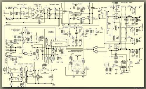
A typical power supply circuit is shown in Fig. 1
Fig. 1 Typical ATX PSU circuit
Checking the high voltage part of the ATX power supply
To begin with, we check: a fuse, a protective thermistor, coils, a diode bridge, high voltage electrolytes, power transistors T2, T4, the primary winding of the transformer, controls in the base circuit of power transistors.
The power transistors usually burn out first. It is better to replace with similar ones: 2SC4242, 2SC3039, KT8127 (A1-B1), KT8108 (A1-B1), etc. Elements in the base circuit of power transistors. (Check resistors for open circuit). As a rule, if the diode bridge burns out (diodes ring shortly), then, accordingly, from the input to the circuit alternating current high voltage electrolytes fly out. Usually the bridge is RS205 (2A 500V) or worse. Recommended - RS507 (5A 700V) or similar. Well, the last fuse is always on.
And so: all non-working elements are replaced. You can start safe testing of the power section of the unit. To do this, you need a transformer with a 36V secondary winding. We connect as shown in Fig. 2. The diode bridge output should have a voltage of 50..52V. Accordingly, each high voltage electrolyte will have half of 50..52V. Between the emitter and collector of each power transistor, there should also be half of 50..52V.
Fig. 2
Checking the standby power supply
The standby power supply is used to power the TL494CN and + 5VSB. As a rule, T11, D22, D23, C30 fail. You should also check the primary and secondary windings of the transformer.
Fig. 3
Checking the control scheme
To do this, you need a stabilized 12V power supply. We connect the tested UPS to the circuit as shown in the diagram in Fig. 1 and look at the presence of oscillograms on the corresponding terminals. Take the oscilloscope readings relative to the common wire.

Fig. 4
Checking power transistors
In principle, you do not need to check the operating modes. If the first two points are passed, then 99% of the power supply unit can be considered serviceable. However, if the power transistors have been replaced with other analogs or if you decide to replace bipolar transistors with field-effect transistors (for example, KP948A, the pinout is the same), then you need to check how the transistor holds transients. To do this, connect the tested unit as shown in Fig. 2. Disconnect the oscilloscope from the common wire! Measure the oscillograms on the collector of the power transistor relative to its emitter (as shown in Fig. 5, the voltage will vary from 0 to 51V). In this case, the process of transition from a low level to a high level should be instantaneous (well, or almost instantaneous), which largely depends on the frequency characteristics of the transistor and damper diodes (in Fig. 5 FR155, analogue 2D253, 2D254). If the transient process occurs smoothly (there is a slight slope), then most likely after a few minutes the radiator of the power transistors will become very hot. (at normal work - the radiator must be cold).

Fig. 5
Checking the output parameters of the power supply
After all the above work, it is necessary to check the output voltages of the unit. Voltage instability under dynamic load, own ripple, etc. You can, at your own peril and risk, stick the unit under test into a working motherboard or assemble a circuit in Fig. 6.
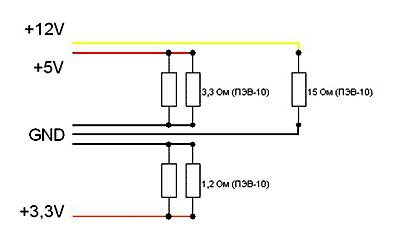
Fig. 6
This circuit is assembled from PEV-10 resistors. Mount resistors on aluminum radiator (channel 20x25x20 is very suitable for these purposes). Do not turn on the power supply unit without a fan! It is also advisable to blow the resistors. Watch the ripple with an oscilloscope directly on the load (from peak to peak should be no more than 100 mV, in the worst case 300 mV). It is generally not recommended to load the power supply unit with more than 1/2 of the declared power (for example: if it is indicated that the power supply unit is 200 watts, then load no more than 100 watts).
In addition to everything written above, I suggest downloading an excellent selection of schematic diagrams of ATX computer power supplies. More than 35 schemes are in the archive. Many manufacturers copy power supplies from each other, so there is a chance to stumble upon the circuit you are looking for. Schematic diagrams Power supply units of such companies as Codegen, Microlab, InWIN, Power Link, JNC, Sunny, and many others. Also in the archive you will find information on the repair of computer power supplies.
You can download the archive with power supply circuits here -
The circuitry of these power supplies is approximately the same for almost all manufacturers. A slight difference applies only to the AT and ATX power supplies. The main difference between the two is that the PSU in the AT does not support the advanced power management standard in software. You can turn off this PSU only by stopping the voltage supply to its input, and in ATX format power supplies there is the possibility of software shutdown by a control signal from the motherboard. As a rule, an ATX board is larger than an AT and is vertically elongated.
General information.
The power supply is implemented in the ATX12V 2.0 format, adapted for the domestic consumer, so it does not have a power switch and a variable network switch. Output connectors include:
connector for connection to the system board - main 24-pin power connector;
4-pin + 12V connector (P4 connector);
removable media power connectors;
nutrition hard disk Serial ATA. It is assumed that the main power connector is
can be easily transformed into 20-pin by discarding the 4-pin group making it compatible with older motherboards. The presence of a 24-pin connector allows for maximum power connector using standard 373.2W terminals.
Operational information about the ATX-350WP4 power supply is given in Table.
| Characteristic | Parameter |
| Appointment | Internal power supply for PC |
| Format | ATX12V 2.0 |
| Maximum power | 350 watts |
| Input network -, V / A | 230/4 |
| AC frequency, Hz | 50 |
| Output voltages, V | +3.3; +5; +12; -12; -5; + 5_SB |
| Dimensions, cm | 15.0x8.6x14.0 |
The set of elements of the structural diagram of the ATX-350WP4 power supply is typical for switching-type power supplies. These include a two-tier line noise suppressor filter, a low-frequency high-voltage rectifier with a filter, main and auxiliary pulse converters, high-frequency rectifiers, an output voltage monitor, protection and cooling elements. A feature of this type of power supply is the presence of a supply voltage at the input connector of the power supply, while a number of elements of the unit are energized, there is voltage at some of its outputs, in particular, at the + 5V_SB outputs. The block diagram of the source is shown in Fig. 1.
Power supply operation.
A rectified mains voltage of about 300 V is supplying power for the main and auxiliary converters. In addition, a supply voltage is supplied from the output rectifier of the auxiliary converter to the control chip of the main converter. In the off state (PS_On signal has a high level) of the power supply, the main converter is in "sleep" mode, in this case the voltage at its outputs is not recorded by the measuring devices. At the same time, the auxiliary converter produces the main converter supply voltage and the + 5B_SB output voltage. This power supply acts as a standby power supply.
The main converter is switched on according to the principle of remote switching, according to which the signal Ps_On becomes equal to the zero potential ( low level voltage) when turning on the computer. According to this signal, the output voltage monitor generates a permission signal for the formation of control pulses of the PWM controller of the main converter of the maximum duration. The main transducer wakes up from sleep mode. From high-frequency rectifiers through appropriate smoothing filters, voltages of ± 12 V, ± 5 V and +3.3 V are supplied to the power supply output.
With a delay of 0.1 ... 0.5 s relative to the appearance of the PS_On signal, but sufficient for the end of transient processes in the main converter and the formation of supply voltages +3.3 V. +5 V, +12 V at the output of the power supply, by a monitor output voltages, the RG signal is generated. (food is normal). P.G. signal is informational, indicating the normal operation of the power supply. It is issued to the motherboard for initial installation and startup of the processor. Thus, the Ps_On signal controls the power supply, and the P.G. responsible for starting the motherboard, both signals are included in the 24-pin connector.
The main converter uses a pulse mode, the converter is controlled from a PWM controller. The duration of the open state of the converter keys determines the voltage value of the output sources, which can be stabilized within the permissible load.
The state of the power supply is monitored by the output voltage monitor. In case of overload or underload, the monitor generates signals that prohibit the operation of the PWM controller of the main converter, putting it into sleep mode.
A similar situation arises under conditions of emergency operation of the power supply associated with short circuits in the load, which are monitored by a special control circuit. To facilitate thermal conditions in the power supply, forced cooling is used, based on the principle of creating negative pressure (release of warm air).
The schematic diagram of the power supply is shown in Fig. 2.
The mains filter and low-frequency rectifier use elements of protection against mains interference, after passing which the mains voltage is rectified by a bridge-type rectifier circuit. Output voltage protection against noise in the alternating current network is carried out by means of a pair of suppressor filter links. The first link is made on a separate board, the elements of which are CX1, FL1, the second link is made up of the elements of the main board of the power supply CX, CY1, CY2, FL1. Elements T, THR1 protect the power supply from short-circuit currents in the load and voltage surges in the input network.
The bridge rectifier is made on diodes B1-B4. Capacitors C1, C2 form a low-frequency network filter. Resistors R2, R3 are elements of the discharge circuit of capacitors C1, C2 when the power is turned off. Varistors V3, V4 limit the rectified voltage in case of line voltage surges above the accepted limits.
The auxiliary converter is connected directly to the output of the mains rectifier and schematically represents a self-oscillating blocking generator. The active elements of the block-king generator are transistor Q1, n-channel field-effect transistor (MOSFET) and transformer T1. The initial gate current of transistor Q1 is generated by resistor R11R12. At the moment of power supply, the blocking process begins to develop, and current begins to flow through the working winding of the transformer T1. The magnetic flux created by this current induces an EMF in the positive feedback winding. In this case, capacitor C7 is charged through the diode D5 connected to this winding, and the transformer is magnetized. The magnetizing current and the charging current of the capacitor C7 lead to a decrease in the gate current of Q1 and its subsequent blocking. Damping of the surge in the drain circuit is carried out by elements R19, C8, D6, the reliable blocking of the transistor Q1 is carried out by the bipolar transistor Q4.
The main converter of the power supply is made according to a push-pull half-bridge circuit ( fig. 3). The power part of the converter is transistorized - Q2, Q3, reversely connected diodes D1, D2 provide protection of the transistors of the converter from "through currents". The second half of the bridge is formed by capacitors C1, C2, which create a rectified voltage divider. The diagonal of this bridge includes the primary windings of the transformers T2 and TZ, the first of them is rectifier, and the second operates in the control circuit and protection against "excessive" currents in the converter. To exclude the possibility of asymmetric biasing of the TZ transformer, which can occur during transient processes in the converter, an isolation capacitor SZ is used. The operating mode of the transistors is set by the elements R5, R8, R7, R9.
The control pulses to the transistors of the converter are fed through the matching transformer T2. However, the start of the converter occurs in a self-oscillating mode, when the transistor 03 is open, the current flows through the circuit:
+ U (B1 ... B4) -\u003e Q3 (k-e) -\u003e T2 - T3 -\u003e C3 -\u003e C2 -\u003e -U (BL..B4).
In the case of an open transistor Q2, current flows through the circuit:
+ U (B1 ... B4) -\u003e C1 -\u003e C3 -\u003e T3 -\u003e T2 -\u003e Q2 (k-e) -\u003e -U (B1 ... B4).
Through the transition capacitors C5, C6 and limiting resistors R5, R7 control signals enter the base of the key transistors, the rejection circuit R4C4 prevents the penetration of impulse noise into the alternating electrical network. Diode D3 and resistor R6 form a discharge circuit of the capacitor C5, and D4 and R10 form a discharge circuit Sb.
When current flows through the primary winding of the TZ, the process of energy accumulation by the transformer occurs, the transfer of this energy to the secondary circuits of the power source and the charge of the capacitors C1, C2. The steady-state mode of operation of the converter will begin after the total voltage across the capacitors C1, C2 reaches +310 V. At the same time, power will appear on the U3 microcircuit (pin 12) from a source made on the elements D9, R20, C15, C16.
The converter is controlled by a cascade based on transistors Q5, Q6 (Fig. 3). The load of the cascade is the symmetrical semi-windings of the transformer T2, at the connection point of which the supply voltage +16 V is supplied through the elements D9, R23. The operating mode of transistors Q5 and Q6 is set by resistors R33, R32, respectively. The cascade is controlled by pulses of the PWM shaper microcircuit U3, coming from pins 8 and 11 to the base of the cascade transistors. Under the influence of control pulses, one of the transistors, for example Q5, opens, and the second, Q6, respectively, closes. Reliable locking of the transistor is carried out by the D15D16C17 chain. So, when current flows through the open transistor Q5 along the circuit:
+ 16V -\u003e D9 -\u003e R23 -\u003e T2 -\u003e Q5 (to-e) -\u003e D15, D16 -\u003e case.
A voltage drop of +1.6 V is formed in the emitter of this transistor. This value is enough to turn off the transistor Q6. The presence of the capacitor C17 helps to maintain the blocking potential during the "pause".
Diodes D13, D14 are designed to dissipate magnetic energy accumulated in the half-windings of the transformer T2.
The PWM controller is based on an AZ7500BP microcircuit (BCD Semiconductor) operating in push-pull mode. The elements of the generator timing circuit are capacitor C28 and resistor R45. Resistor R47 and capacitor C29 form an error amplifier correction circuit 1 ( fig. 4).
To implement the push-pull mode of the converter operation, the control input of the output stages (pin 13) is connected to a reference voltage source (pin 14). From pins 8 and 11 of the microcircuit, control pulses enter the base circuits of the transistors Q5, Q6 of the control cascade. Voltage +16 V is supplied to the microcircuit power output (pin 12) from the auxiliary converter rectifier.
The "slow start" mode is implemented using an error amplifier 2, the non-inverting input of which (pin 16 U3) receives a supply voltage of +16 V through the divider R33R34R36R37C21, and the inverting input (pin 15) receives a voltage from the reference source (pin 14 ) from the integrating capacitor C20 and the resistor R39.
The sum of voltages of +12 V and +3.3 V is supplied to the non-inverting input of the error amplifier 1 (pin 1 U3) through the adder R42R43R48. The voltage from the reference source of the microcircuit is supplied to the opposite input of the amplifier (pin 2 U3) through the divider R40R49 from the reference source of the microcircuit (pin. 14 U3). Resistor R47 and capacitor C29 are frequency correction elements of the amplifier.
Stabilization and protection chains. The duration of the output pulses of the PWM controller (pin. 8, 11 U3) in the steady state is determined by the feedback signals and the sawtooth voltage of the master oscillator. The time interval during which the "saw" exceeds the feedback voltage determines the duration of the output pulse. Let's consider the process of their formation.
From the output of the error amplifier 1 (pin 3 U3), information about the deviation of the output voltages from the nominal value in the form of a slowly varying voltage is fed to the PWM driver. Further, from the output of the error amplifier 1, the voltage is supplied to one of the inputs of the pulse-width modulator (PWM). Its second input receives a sawtooth voltage with an amplitude of +3.2 V. Obviously, when the output voltage deviates from the nominal values, for example, downward, the feedback voltage will decrease at the same value of the sawtooth voltage supplied to the pin. 1, which leads to an increase in the duration of the output pulse cycles. In this case, more electromagnetic energy is accumulated in the transformer T1, which is given to the load, as a result of which the output voltage rises to the nominal value.
In the emergency mode of operation, the voltage drop across the resistor R46 increases. At the same time, the voltage at pin 4 of the U3 microcircuit increases, and this, in turn, leads to the operation of the "pause" comparator and a subsequent decrease in the duration of the output pulses and, accordingly, to limiting the flow of current through the transistors of the converter, thereby preventing the output of Q1, Q2 from building.
The source also has short-circuit protection circuits in the output voltage channels. The short-circuit sensor on channels -12 V and -5 V is formed by elements R73, D29, the midpoint of which is connected to the base of the transistor Q10 through a resistor R72. Here, through the resistor R71, the voltage from the +5 V source is supplied. Therefore, the presence of a short circuit in the -12 V (or -5 V) channels will lead to the unlocking of the Q10 transistor and an overload on pin 6 of the voltage monitor U4, and this, in turn, will stop the converter on pin 4 of the converter U3.
Power supply control, monitoring and protection. Almost all computers, in addition to high-quality performance of its functions, require easy and quick on / off. The task of turning on / off the power source is solved by implementing the principle of remote on / off in modern computers. When you press the "I / O" button located on the front panel of the computer case, the processor board generates the PS_On signal. To turn on the power supply, the PS_On signal must have a low potential, i.e. zero, when turned off - high potential.
In the power supply, the tasks of control, monitoring and protection are implemented on the U4 microcircuit of the output voltage monitor of the LP7510 power supply. When a zero potential (PS_On signal) arrives at pin 4 of the microcircuit, a zero potential is also formed at pin 3 with a delay of 2.3 ms. This signal is the trigger for the power supply. If the PS_On signal is high or its input circuit is broken, then pin 3 of the microcircuit is also set to a high level.
In addition, the U4 microcircuit monitors the main output voltages of the power supply. So, the output voltages of 3.3 V and 5 V power supplies should not go beyond the established limits of 2.2 V< 3,3В < 3,9 В
и 3,5 В < 5 В < 6,1 В. В случае их выхода за эти пределы более
чем на 146 мкс на выходе 3 микросхемы U4 устанавливается высокий уровень
напряжения, и источник питания выключается по входу 4 микросхемы U3.
Для источника питания +12 В, контролируемого по выводу 7, существует
только контроль над его превышением. Напряжение питания этого источника
не должно превышать больше чем 14,4 В. В перечисленных emergency modes the main converter goes into sleep mode by setting a high voltage at pin 3 of the U4 microcircuit. In this way, the control and protection of the power supply unit against a decrease and increase in voltage at the outputs of its main sources ( fig. 5).
In all cases of a high voltage level at pin 3, the voltage at pin 8 is normal, PG is low (zero). In the case when all supply voltages are normal, a low level of the PSOn signal is set at pin 4, and a voltage not exceeding 1.15 V is present at pin 1, a high level signal appears at pin 8 with a delay of 300 ms.
The thermoregulation circuit is designed to maintain temperature regime inside the power supply case. The circuit consists of a fan and a THR2 thermistor, which are connected to the + 12V channel. constant temperature inside the case is achieved by adjusting the speed by rotating the fan.
Pulse voltage rectifiers use a typical full-wave midpoint rectifier circuit to provide the required ripple ratio.
The rectifier of the power supply +5 V_SB is made on the diode D12. The two-tier output voltage filter consists of a capacitor C15, an inductor L3 and a capacitor C19. Resistor R36 is a load resistor. This voltage is stabilized by microcircuits U1, U2.
The +5 V power supply is made on the D32 diode assembly. The two-link filter of the output voltage is formed by the winding L6.2 of a multi-winding choke, choke L10, capacitors C39, C40. Resistor R69 is a load resistor.
The +12 V power supply is made in the same way. Its rectifier is implemented on the D31 diode assembly. The two-link filter of the output voltage is formed by the winding L6.3 of a multi-winding choke, choke L9, capacitor C38. Power supply load - thermoregulation circuit.
Voltage rectifier +3.3 V - diode assembly D30. The circuit uses a parallel type regulator with a regulating transistor Q9 and a parametric regulator U5. The voltage is supplied to the control input U5 from the divider R63R58. Resistor R67 is the load of the divider.
To reduce the level of interference emitted by pulse rectifiers into the electrical network, resistive-capacitive filters on the elements R20, R21, СЮ, С11 are connected in parallel to the secondary windings of the transformer T1.
Power supplies of negative voltages -12 V, -5 V are formed in the same way. So for a 12 V source, the rectifier is made on diodes D24, D25, D26, smoothing filter L6.4L5C42, resistor R74 - load.
Voltage -5 V is generated by diodes D27, 28. The filters of these sources are -L6.1L4C41. Resistor R75 is a load resistor.

Typical malfunctions
Mains fuse T blown or no output voltages. In this case, it is necessary to check the health of the elements of the barrier filter and the network rectifier (B1-B4, THR1, C1, C2, V3, V4, R2, R3), and also check the health of the transistors Q2, Q3. Most often, if the wrong AC network is selected, the varistors V3, V4 burn out.
The serviceability of the elements of the auxiliary converter, transistors Q1.Q4 is also checked.
If the malfunction is not detected and the failure and operation of the previously considered elements was not confirmed, then the presence of a voltage of 310 V on the series-connected capacitors C1, C2 is checked. In its absence, the serviceability of the network rectifier elements is checked.
Voltage + 5 \\ / _ ZV is higher or lower than normal. Check the stability of the stabilization circuit U1, U2, the faulty element is replaced. TL431, КА431 can be used as a replacement element for U2.
Output supply voltages are higher or lower than normal. We check the serviceability of the feedback circuit - the U3 microcircuit, the U3 microcircuit strapping elements: capacitors C21, C22, C16. Replace U3 if the above elements are working properly. The chips TL494, KA7500V, MV3759 can be used as U3 analogs.
P.G. signal missing Check the presence of the Ps_On signal, the presence of supply voltages +12 V, +5 V, +3.3 V, +5 B_SB. If available, replace the U4 microcircuit. TPS3510 can be used as an analogue of LP7510.
There is no remote power supply activation. Check the presence of the housing potential (zero) on the PS-ON contact, the serviceability of the U4 microcircuit and its trim elements. If the trim elements are in good condition, replace U4.
No fan rotation. Make sure that the fan is working, check the elements of its switching circuit: the presence of +12 V, the serviceability of the THR2 thermistor. The article provides information on circuit solutions, recommendations for repair, replacement of analog parts of the ATX-350WP4 power supply
A fairly common defect, with exotic reasons. A whistle is heard in standby mode. The source of the whistle is a damper capacitor in the collector (drain) of the standby source transistor. For ceramics, the piezoelectric effect is inherent, which increases over time. Along with a defective capacitor, there is often a leak at the damper diode. To drastically reduce the whistle and increase the reliability of the power supply, the components must be replaced with FR207 and a capacitor of the same capacity for a voltage of at least 1 kV. The capacitor may not be ceramic.
D. Kucherov, Radioamator magazine, No. 3, 5 2011
An integral part of every computer is power supply unit (PSU)... It is as important as the rest of the computer. At the same time, the purchase of a power supply unit is carried out quite rarely, since a good power supply unit can provide power for several generations of systems. Considering all this, the purchase of a power supply unit must be taken very seriously, since the fate of a computer is directly dependent on the operation of the power supply unit.
The main purpose of the power supply issupply voltage generation, which is necessary for the functioning of all PC units. The main component supply voltages are:
- + 12V
- + 3.3V
There is also additional stress:
- −12V
To implement galvanic isolation it is enough to make a transformer with the necessary windings. But to power the computer you need a lot power, especially for modern PCs... For computer power it would be necessary to make a transformer that would not only be large, but also very heavy. However, with an increase in the frequency of the supply current of the transformer, to create the same magnetic flux, fewer turns and a smaller section of the magnetic circuit are required. In power supplies based on a converter, the frequency of the supply voltage of the transformer is 1000 or more times higher. This allows the creation of compact and lightweight power supplies.
The simplest pulse power supply
Consider a block diagram of a simple switching power supply, which is at the heart of all switching power supplies.
.
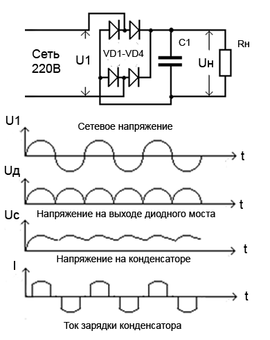
The first block carries out conversion of AC mains voltage to DC... Such converterconsists of a diode bridge that rectifies the alternating voltage, and a capacitor that smooths the ripple of the rectified voltage. This bokeh also contains additional elements: mains voltage filters from the pulsation of the pulse generator and thermistors for smoothing the current surge at the moment of switching on. However, these items may not be available in order to save on cost.
The next block is pulse generator, which generates pulses at a certain frequency that feed the primary winding of the transformer. The frequency of generating pulses of different power supplies is different and lies in the range of 30-200 kHz. The transformer performs the main functions of the power supply unit: galvanic isolation from the mains and voltage reduction to the required values.
The alternating voltage received from the transformer is converted by the next unit into constant pressure... The unit consists of voltage rectifying diodes and a ripple filter. In this block, the ripple filter is much more complicated than in the first block and consists of a group of capacitors and a choke. In order to save money, manufacturers can install low-capacity capacitors, as well as low-inductance chokes.
The first impulse power block was push-pull or single-pull converter... Push-pull means that the generation process has two parts. In such a converter, two transistors open and close in turn. Accordingly, in a single-ended converter, one transistor opens and closes. The diagrams of push-pull and single-pull converters are presented below.

.
Let's consider the elements of the scheme in more detail:
X2 - power supply connector for the circuit.
X1 - connector from which the output voltage is removed.
R1 - resistance that sets the initial small offset on the keys. It is necessary for a more stable start of the oscillation process in the converter.
R2 is the resistance that limits the base current on the transistors, this is necessary to protect the transistors from combustion.
TP1 - The transformer has three groups of windings. The first output winding forms the output voltage. The second winding serves as a load for the transistors. The third generates the control voltage for the transistors.
At the initial moment of turning on the first circuit, the transistor is slightly open, since a positive voltage is applied to the base through the resistor R1. A current flows through the slightly open transistor, which also flows through the II winding of the transformer. The current flowing through the winding creates a magnetic field. The magnetic field creates a voltage in the rest of the transformer windings. As a result, a positive voltage is created on winding III, which opens the transistor even more. The process continues until the transistor reaches saturation mode. The saturation mode is characterized by the fact that with an increase in the applied control current to the transistor, the output current remains unchanged.
Since the voltage in the windings is generated only in the event of a change in the magnetic field, its growth or fall, the absence of an increase in current at the output of the transistor, therefore, will lead to the disappearance of the EMF in windings II and III. A voltage drop in winding III will lead to a decrease in the degree of opening of the transistor. And the output current of the transistor will decrease, therefore, the magnetic field will also decrease. Decreasing the magnetic field will create a voltage of opposite polarity. The negative voltage in winding III will begin to close the transistor even more. The process will continue until the magnetic field completely disappears. When the magnetic field disappears, the negative voltage in winding III will also disappear. The process will start repeating again.
A push-pull converter works on the same principle, but the difference is that there are two transistors, and they open and close in turn. That is, when one is open, the other is closed. The push-pull converter circuit has a great advantage, since it uses the entire hysteresis loop of the magnetic conductor of the transformer. The use of only one section of the hysteresis loop or magnetization in only one direction leads to the occurrence of many undesirable effects that reduce the efficiency of the converter and degrade its characteristics. Therefore, basically everywhere a push-pull converter circuit with a phase-shifting transformer is used. In circuits where simplicity, small dimensions, and low power are needed, a single-ended circuit is still used.
ATX form factor power supplies without power factor correction
The converters discussed above, although complete devices, are inconvenient to use in practice. The frequency of the converter, the output voltage and many other parameters "float", change depending on changes: supply voltage, load of the converter output and temperature. But if the keys are controlled by a controller that could carry out stabilization and various additional functionsthen you can use the circuit to power the devices. The power supply circuit using a PWM controller is quite simple, and, in general, is a pulse generator built on a PWM controller.
PWM - pulse width modulation... It allows you to adjust the amplitude of the transmitted low-pass filter (low-pass filter) with a change in the duration or duty cycle. The main advantages of PWM are the high efficiency of power amplifiers and great application possibilities.

This power supply circuit has a low power and uses a field-effect transistor as a key, which allows you to simplify the circuit and get rid of additional elements necessary to control transistor keys. AT high power power supplies PWM controller has control elements ("Driver") for the output key. IGBT transistors are used as output switches in high-power power supplies.
The mains voltage in this circuit is converted into a constant voltage and through the key goes to the first winding of the transformer. The second winding is used to power the microcircuit and form the feedback voltage. The PWM controller generates pulses with a frequency set by the RC circuit connected to leg 4. The pulses are fed to the input of the key, which amplifies them. The duration of the pulses changes depending on the voltage at the leg 2.
Consider a real ATX power supply circuit. It has many more elements and contains more additional devices... The power supply circuit is conventionally divided into main parts by red squares.

ATX circuit of a power supply unit with a capacity of 150-300 W
To power the controller microcircuit, as well as to generate a standby voltage +5, which is used by the computer when it is turned off, there is another converter in the circuit. In the diagram, it is designated as block 2. As you can see, it is made according to the scheme of a single-cycle converter. The second block also has additional elements. Basically, these are voltage surge absorption chains that are generated by the converter transformer. Microcircuit 7805 - the voltage stabilizer generates a standby voltage of + 5V from the rectified voltage of the converter.
Often, substandard or defective components are installed in the standby voltage generation unit, which causes a decrease in the frequency of the converter to the audio range. As a result, a squeak is heard from the power supply.
Since the power supply is powered by an AC voltage 220V, and the converter needs a constant voltage supply, the voltage needs to be converted. The first block rectifies and filters the alternating mains voltage. This block also contains a suppression filter against noise generated by the power supply itself.
The third block is a PWM controller TL494 ... It performs all the main functions of the power supply. Protects the power supply from short circuits, stabilizes output voltages and generates a PWM signal to control transistor switches that are loaded on a transformer.
The fourth block consists of two transformers and two groups of transistor switches. The first transformer generates the control voltage for the output transistors. Since the PWM controller TL494 generates a low power signal, the first group of transistors amplifies this signal and transmits it to the first transformer. The second group of transistors, or output transistors, are loaded onto the main transformer, which forms the main supply voltages. Such a more complex circuit for controlling the output switches is used due to the complexity of controlling bipolar transistors and protecting the PWM controller from high voltage.
The fifth block consists of Schottky diodes, which rectify the output voltage of the transformer, and a low-pass filter (LPF). Low-pass filter consists of electrolytic capacitors of significant capacity and chokes. At the output of the low-pass filter there are resistors that load it. These resistors are necessary so that after turning off the capacity of the power supply unit does not remain charged. There are also resistors at the output of the mains voltage rectifier.
The remaining elements not circled in the block are chains, form " health signals". These chains are used to protect the power supply from short circuits or to monitor the health of the output voltages.

Now let's see how on the printed circuit board 200 W power supply the elements are arranged. The figure shows:
Capacitors that filter the output voltages.
Place of unsoldered capacitors of the output voltage filter.
Inductors that filter the output voltages. The larger coil not only plays the role of a filter, but also works as a ferromagnetic stabilizer. This allows you to slightly reduce voltage imbalances with uneven loading of different output voltages.
Chip PWM stabilizer WT7520.
A radiator on which Schottky diodes are installed for voltages + 3.3V and + 5V, and for a voltage of + 12V, ordinary diodes. It should be noted that often, especially in old power supplies, additional elements are placed on the same radiator. These are voltage stabilization elements + 5V and + 3.3V. AT modern blocks power supply is placed on this radiator only Schottky diodes for all main voltages or field-effect transistors, which are used as a rectifier element.
The main transformer, which forms all voltages, as well as galvanic isolation from the network.
A transformer that generates control voltages for the output transistors of the converter.
Converter transformer that generates a standby voltage of + 5V.
A radiator on which the output transistors of the converter are located, as well as the transistor of the converter that forms the standby voltage.
Line voltage filter capacitors. It doesn't have to be two. To form a bipolar voltage and form a midpoint, two capacitors of equal capacity are installed. They divide the rectified mains voltage in half, thereby forming two voltages of different polarity, connected at a common point. In circuits with a unipolar supply, there is one capacitor.
Elements of the mains filter from harmonics (interference) generated by the power supply.
Diodes of a diode bridge that rectify the alternating voltage of the network.
Power supply 350 W is arranged equivalently. Immediately striking is the large board, enlarged heat sinks and a larger converter transformer.
Output voltage filter capacitors.
Radiator, cooling diodes, rectifying the output voltage.
PWM controller AT2005 (analogue of WT7520), which stabilizes voltages.
Main transformer of the converter.
A transformer that generates a control voltage for the output transistors.
Standby voltage converter transformer.
A radiator that cools the output transistors of the converters.
Line voltage filter from power supply noise.
Diode bridge diodes.
Line voltage filter capacitors.
The considered scheme has been used for a long time in power supplies and is now sometimes found.
ATX power supplies with power factor correction
In the considered circuits, the network load is a capacitor connected to the network through a diode bridge. The capacitor is charged only if the voltage on it is less than the mains voltage. As a result, the current is pulsed, which has many disadvantages.
Let's list these disadvantages:
- currents introduce higher harmonics (noise) into the network;
- large amplitude of current consumption;
- significant reactive component in the current consumption;
- the mains voltage is not used during the entire period;
- The efficiency of such circuits is of little importance.
New power supplies have an improved modern circuit, one more additional block has appeared in it - power factor corrector (PFC)... It realizes power factor improvement. Or, in simpler terms, it removes some of the disadvantages of the mains voltage bridge rectifier.
S \u003d P + jQ
Formula full power
Power factor (KM) characterizes how much active component is in full power and how much is reactive. In principle, we can say, why take into account reactive power, it is imaginary and does not benefit.

Let's say we have a certain device, a power supply, with a power factor of 0.7 and a power of 300 watts. It can be seen from the calculations that our power supply has a total power (the sum of reactive and active power) more than that indicated on it. And this power should be provided by the 220V power supply network. Although this power is not useful (even the electricity meter does not register it), it still exists.
That is, the internal elements and mains wires must be rated for 430 W, not 300 W. Imagine a case where the power factor is 0.1 ... Because of this, the GORSETYU is prohibited from using devices with a power factor less than 0.6, and if such is found, the owner is fined.
Accordingly, the campaigns developed new power supply circuits that had KKM. Initially, a large inductance choke included at the input was used as a PFC, such a power supply is called a power supply with PFC or passive PFC. Such a power supply unit has an increased KM. To achieve the desired CM, it is necessary to equip the power supplies with a large choke, since the input resistance of the power supply is of a capacitive nature due to the installed capacitors at the output of the rectifier. Installing a choke significantly increases the mass of the power supply, and increases the KM to 0.85, which is not so much.

The figure shows the company's power supply FSP 400 W with passive power factor correction. It contains the following elements:
- Output voltage ripple filter capacitors.
Rectified mains voltage filter capacitors.
Power factor correction choke.
Main converter transformer.
Key transformer.
Auxiliary converter transformer (standby voltage).
Line voltage filters from power supply ripple.
A radiator on which the output transistor switches are installed.
A radiator on which diodes are installed that rectify the alternating voltage of the main transformer.
Fan speed control board.
The board on which the FSP3528 PWM controller is installed (analogous to the KA3511).
Group stabilization choke and output voltage ripple filter elements.

Due to the low efficiency of the passive PFC, a new PFC circuit was introduced into the power supply, which is built on the basis of a PWM stabilizer loaded onto a choke. This circuit brings many advantages to the power supply:
- extended range of operating voltages;
- it became possible to significantly reduce the capacitance of the mains voltage filter capacitor;
- significantly increased BM;
- reducing the mass of the power supply;
- increase in the efficiency of the power supply.
There are also disadvantages to this scheme - these are decrease in power supply reliability and incorrect work with some uninterruptible power suppliesi when switching between battery / mains operating modes. Incorrect operation of this circuit with a UPS is caused by the fact that the capacity of the mains voltage filter in the circuit has significantly decreased. At the moment when the voltage disappears for a short time, the current of the KKM increases greatly, which is necessary to maintain the voltage at the output of the KKM, as a result of which the protection against short circuit (short circuit) in the UPS is triggered.

If you look at the circuit, then it is a pulse generator that is loaded onto the inductor. The mains voltage is rectified by a diode bridge and fed to the switch, which is loaded with a choke L1 and a transformer T1. The transformer is introduced for the feedback of the controller with the key. The choke voltage is removed using diodes D1 and D2. Moreover, the voltage is removed alternately with the help of diodes, then from the diode bridge, then from the inductor, and charges the capacitors Cs1 and Cs2. The Q1 switch opens and the required energy is accumulated in the L1 throttle. The amount of accumulated energy is regulated by the duration of the key open state. The more energy is stored, the more voltage the choke will give. After turning off the key, the accumulated energy is returned by the choke L1 through the diode D1 to the capacitors.
This work allows you to use the entire sinusoidal AC voltage of the network in contrast to circuits without PFC, as well as stabilize the voltage supplying the converter.
AT modern schemes power supplies are often used dual channel PWM controllers... One microcircuit carries out the work of both the converter and the KKM. As a result, the number of elements in the power supply circuit is significantly reduced.

Consider a simple 12V power supply circuit using a ML4819 dual-channel PWM controller. One part of the power supply forms a constant stabilized voltage + 380V. The other part is a converter that generates a constant stabilized voltage of + 12V. KKM consists, as in the above considered case, of the key Q1, the choke L1 of the feedback transformer T1 loaded on it. Diodes D5, D6 charge capacitors C2, ° C3, ° C4. The converter consists of two switches Q2 and Q3, loaded on the transformer T3. Impulse voltage rectified by diode assembly D13 and filtered by choke L2 and capacitors C16, ° C18. With the help of the U2 cartridge, the output voltage regulation voltage is generated.

Consider the design of the power supply unit, which has an active PFC:
- Current protection control board;
- Choke that acts as both a voltage filter of + 12V and + 5V, and a group stabilization function;
- Voltage filter choke + 3.3V;
- A radiator on which the rectifier diodes of output voltages are located;
- Main converter transformer;
- Transformer controlling the keys of the main converter;
- Auxiliary converter transformer (generating standby voltage);
- Power factor correction controller board;
- Radiator, cooling diode bridge and main converter keys;
- Mains voltage filters from interference;
- Power factor corrector choke;
- Line voltage filter capacitor.
Design features and types of connectors
Consider types of connectorsthat may be present on the power supply. On the back of the power supply the connector for connection is located network cable and a switch. Previously, there was also a connector for the monitor's network cable next to the power cord connector. Other elements may optionally be present:
- indicators of mains voltage, or the status of the power supply
- fan control buttons
- button for switching the input mains voltage 110 / 220V
- USB ports built into the USB hub power supply
- other.

Fans are less and less often placed on the rear wall, drawing air from the power supply. The fan is placed more and more at the top of the PSU due to the larger space for the fan, which allows the installation of a large and quiet active cooling element. Some power supplies even have two fans on top and back.

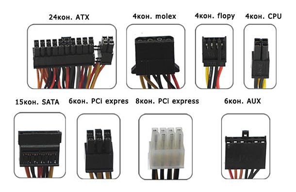
From the front wall comes wire with motherboard power connector... In some power supplies, modular, it, like other wires, is connected via a connector. The figure below shows pinout of contacts of all main connectors .

You can see that each voltage has a different wire color:
- Yellow color - +12 V
- Red color - +5 V
- Orange color - + 3.3V
- Black is common or ground
For other voltages, the wire colors may vary for each manufacturer.
The figure does not show the additional power connectors for video cards, since they are similar to the additional power connector for the processor. There are also other types of connectors that are found in branded computers from DelL, Apple and others.
Electrical parameters and characteristics of power supplies
The power supply has many electrical parameters, most of which are not indicated in the passport. On the side sticker of the power supply, usually only a few basic parameters are noted - operating voltages and power.
Power supply power
Power is often indicated on the label in large print. The power of the power supply characterizes how much it can give off electrical energy to the devices connected to it (motherboard, video card, hard drive, etc.).
In theory, it is enough to sum up the consumption of the components used and choose a power supply unit a little more power for the stock. For calculating power the recommendations given in the passport of the video card, if there is one, CPU thermal package, etc.
But in fact, everything is much more complicated, since the power supply provides various voltages - 12V, 5V, −12V, 3.3V, etc. Each voltage line is designed for its own power. It was logical to think that this power is fixed, and their sum is equal to the power of the power supply. But in the power supply there is one transformer for generating all these voltages used by the computer (except for the standby voltage of + 5V). True, rarely, but you can still find a power supply with two separate transformers, but such power supplies are expensive and are most often used in servers. Conventional ATX PSUs have one transformer. Because of this, the power of each stress line can float: it increases if other lines are weakly loaded, and decreases if the other lines are heavily loaded. Therefore, the maximum power of each line is often written on the power supplies, and as a result, if they are summed up, the power will be released even more than the actual power of the power supply. Thus, the manufacturer can confuse the consumer, for example, by declaring too high a rated power that the PSU is not capable of providing.
Note that if the computer has insufficient power supply, then this will cause incorrect operation of devices ( Freezes, reboots, clicking of the hard disk heads), up to the impossibility turning on the computer... And if a motherboard is installed in a PC that is not designed for the power of the components that are installed on it, then the motherboard often functions normally, but over time, the power connectors burn out due to their constant heating and oxidation.

Standards and certifications
When buying a power supply unit, first of all, you need to look at the availability of certificates and its compliance with modern international standards. On power supplies, the following standards are most often found:
There are also computer standards for the ATX form factor, which defines the dimensions, design and many other parameters of the power supply, including the permissible voltage tolerances under load. Today there are several versions of the ATX standard:
- ATX 1.3 Standard
- ATX 2.0 Standard
- ATX 2.2 Standard
- ATX 2.3 Standard
The difference between the versions of ATX standards mainly concerns the introduction of new connectors and new requirements for the power supply lines of the power supply.
Recommendations for choosing a power supply
When arises the need to purchase a new power supply ATX, then first you need to determine the power that is needed to power the computer in which this power supply will be installed. To determine it, it is enough to sum up the capacities of the components used in the system, for example, using a special calculator. If this is not possible, then we can proceed from the rule that for an average computer with one gaming video card, a power supply with a capacity of 500-600 watts is enough.
Considering that most of the parameters of power supplies can be found out only by testing it, the next step is strongly recommend that you familiarize yourself with the tests and reviews of possible applicants - power supply modelsthat are available in your region and satisfy your needs at least in terms of the provided capacity. If this is not possible, then it is necessary to choose according to the compliance of the power supply unit with modern standards (the larger the number, the better), while the presence of the ACKM circuit (APFC) in the power supply unit is desirable. When purchasing a power supply, it is also important to turn it on, if possible, right at the place of purchase or immediately upon arrival at home, and monitor how it works so that the power supply does not emit squeaks, hums or other extraneous noise.
In general, it is necessary to choose a power supply unit that would be powerful, of high quality, with good declared and real electrical parameters, as well as it would be convenient to use and quiet during operation, even with a high load on it. And in no case should you save a couple of dollars when buying a power supply. Remember that the stability, reliability and durability of the entire computer depends mainly on the operation of this device.